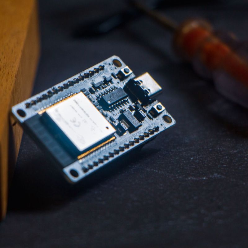
Custom Hardware Platforms Built for Your Application
At AIOTHUB, we design embedded hardware from scratch — selecting the optimal microcontroller architecture, defining power domains, and creating production-grade schematics that meet your exact application requirements.
Whether you need a compact sensor node, an industrial controller, or a complex multi-interface gateway, our hardware engineers bring deep expertise in ARM Cortex-M, RISC-V, ESP32, and STM32 platforms to deliver designs that are reliable, cost-optimized, and ready for volume manufacturing.
Every design goes through rigorous review cycles — design rule checks, signal integrity simulations, and thermal analysis — before we release it for prototyping. This disciplined process eliminates costly re-spins and gets your product to market faster.
Benefits of Our Hardware Design Service
Every hardware design decision is driven by reliability, manufacturability, and your product's long-term success.
Purpose-Built Architecture
No off-the-shelf compromises. We design the entire hardware architecture around your exact functional, power, and form-factor requirements.
Optimized Power Design
Efficient power management with multi-rail supply design, battery management ICs, and ultra-low-power sleep modes for field-deployed devices.
Industrial-Grade Reliability
Wide temperature range, ESD protection, EMI filtering, and conformal coating readiness for harsh industrial environments.
BOM Cost Optimization
Strategic component selection balancing performance, availability, and cost — with second-source alternatives to protect your supply chain.
DFM-Ready Output
Every design is optimized for manufacturability from day one — proper pad sizing, panelization considerations, and assembly-friendly layouts.
Fast Turnaround
Structured design workflow with clear milestones. Most schematic designs are completed within 2–4 weeks depending on complexity.
How We Deliver Your Hardware Design
A structured engineering workflow that takes your concept from requirements to production-ready outputs.
Requirements Analysis
We study your application needs — interfaces, power constraints, environmental specs, and target cost — to define the hardware architecture.
Schematic Design
Complete schematic capture with component selection, power tree design, and signal routing. Formal design review before PCB phase.
Prototype Build
Rapid-turn prototype PCBs are assembled and brought up in our lab. Functional testing validates every subsystem against specifications.
Production Handoff
Finalized Gerbers, BOM, assembly drawings, and test procedures are packaged for seamless handoff to your manufacturing partner.
Embedded Hardware Design FAQs
Answers to the questions our clients ask most before starting a hardware design project.
We work across a wide range of platforms including ARM Cortex-M (STM32, NXP LPC), ESP32/ESP8266, RISC-V, TI MSP430, and Nordic nRF series. We select the optimal MCU based on your application's processing, power, connectivity, and cost requirements.
A typical embedded hardware design takes 4–8 weeks from requirements to prototype-ready output, depending on complexity. Simple sensor boards may take 2–3 weeks, while complex multi-interface gateways can take 8–12 weeks including review cycles.
Yes. We offer end-to-end hardware design covering schematic capture, component selection, PCB layout, and production file generation. We can also work with your existing schematic and handle only the PCB layout if needed.
Absolutely. We have deep experience designing for wide temperature ranges (-40°C to +85°C), high vibration, EMI/EMC compliance, IP65+ enclosures, and conformal coating. Industrial reliability is a core strength.
Yes. We manage the complete prototype cycle — PCB fabrication, component sourcing, SMT assembly, and functional testing. You receive fully assembled and tested prototype boards ready for firmware development and validation.
You do. All design files, schematics, Gerbers, and documentation are delivered to you with full IP ownership. We operate as your engineering partner, not a product company.
Ready to Design Your Custom Hardware?
Tell us about your project requirements and our embedded hardware engineers will get back to you with a free consultation and project estimate.