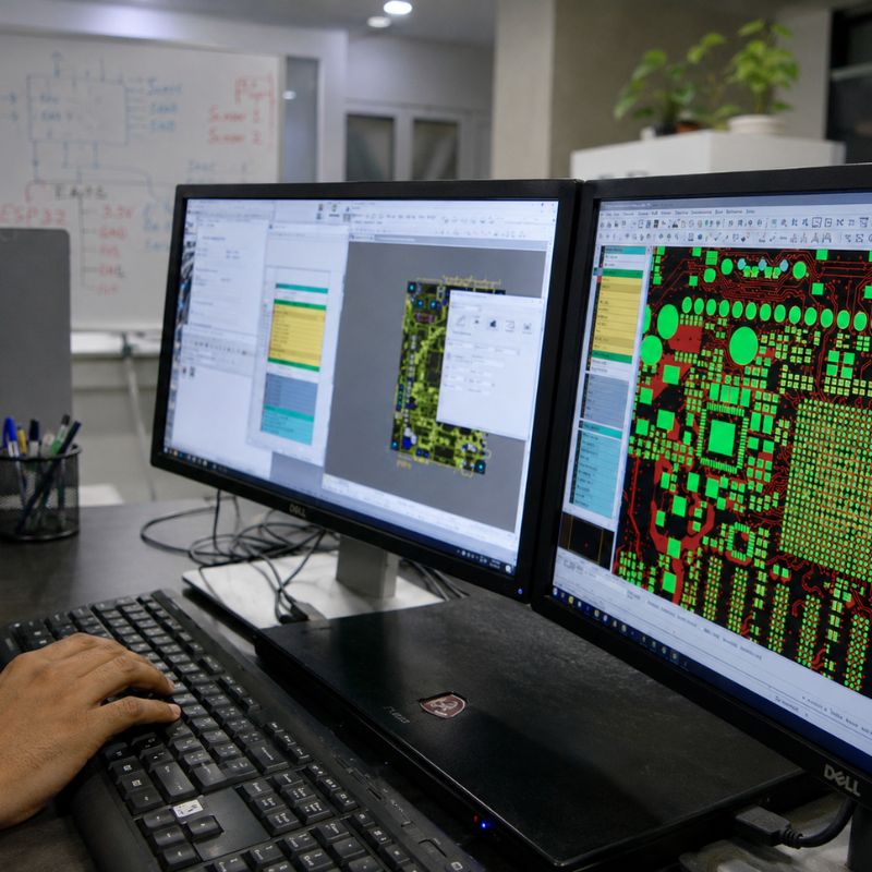
Precision PCB Layout for Every Application
Our PCB layout engineers transform your schematics into production-optimized board designs. We handle the full spectrum — from simple 2-layer single-sided boards to complex 8–12 layer high-density interconnect (HDI) designs with controlled impedance routing and blind/buried vias.
We work with industry-standard EDA tools including Altium Designer, KiCad, and Eagle, and deliver fabrication-ready output that any PCB manufacturer can produce. Every design undergoes DRC, signal integrity analysis, and thermal simulation before release.
Whether you're designing a compact wearable, a high-speed digital processor board, or a mixed-signal industrial controller, we ensure your PCB layout meets both electrical performance requirements and manufacturing constraints.
PCB Design Excellence
Layout quality directly impacts your product's performance, reliability, and manufacturing yield.
Signal Integrity Analysis
Impedance-controlled routing, length matching, differential pair management, and crosstalk minimization for high-speed digital designs.
Thermal Management
Strategic copper pours, thermal vias, and heat sink pad design to keep components within safe operating temperatures.
DFM Optimization
Design for manufacturability — proper pad sizing, solder mask clearances, panelization, and assembly-friendly component placement.
Compact High-Density Layouts
Space-constrained designs with fine-pitch BGA, QFN packages, and HDI technology for miniaturized products.
Mixed-Signal Expertise
Proper analog/digital domain separation, ground plane management, and noise isolation for mixed-signal designs.
RF & Antenna Layout
RF trace routing, impedance matching networks, antenna keep-out zones, and ground plane optimization for wireless designs.
PCB Design Workflow
A systematic approach that ensures first-pass success and eliminates costly re-spins.
Schematic Review
Thorough review of your schematic for design intent, component footprints, and electrical constraints before starting layout.
Stackup & Floorplan
Define layer stackup, board outline, mounting holes, connector placement, and critical component positioning.
Routing & Verification
Complete trace routing with DRC checks, signal integrity analysis, and design review. Iterative refinement until all constraints are met.
Output & Fabrication
Generate Gerber files, drill files, pick-and-place data, and assembly drawings. Ready for any PCB fabricator worldwide.
PCB Design FAQs
We design PCBs from 1-layer to 12+ layers. Most of our industrial and IoT designs are 4–6 layers. For high-speed digital or complex mixed-signal applications, we work with 8–12 layer stackups with controlled impedance.
We primarily work with Altium Designer and KiCad. We can also work with Eagle, OrCAD/Allegro, and PADS. If you have a preferred tool, we'll align with your workflow.
Yes. Provide your schematic in any standard format and we'll handle the PCB layout. We start with a thorough schematic review to catch any issues before layout begins.
Simple 2-layer boards take 3–5 days. Standard 4-layer designs take 1–2 weeks. Complex multi-layer boards with high-speed or RF requirements typically take 2–4 weeks including review cycles.
Yes. We can coordinate directly with your preferred PCB manufacturer or recommend trusted fabrication partners in India and Asia. We handle DFM review feedback and ensure smooth production handoff.
Need a PCB Layout for Your Project?
Share your schematic and requirements — we'll respond with a detailed timeline and quote for your PCB design.